IoT-Inspired Custom PCB Design
One common route for prototyping is buying devices like Raspberry Piand such. Those boards and kits are quite OK for checking out what functionalities could be realized in a prospective commercial product but they (I’m not talking about Compute Modules) rarely ever become part of any actual, final consumer product, for a reason.
There’s absolutely no need to explain this to electronics experts but some having specific interest in non-professional prototyping (and IoT is a massively attractive topic for enthusiasts) might find the below hints useful.
Hardware Footprint
Looking at the hardware side, a consumer product should not be more complicated than necessary. Raspberry Pi comes with a microprocessor, memory of multiple kinds, a rich GPIO header and several options for human-machine interfacing, USB ports, Ethernet, etc. Additionally, it can be sensitive to power outages (without properly addressing such risks).
This might inspire you to minify the overall footprint of your product. This begins with a schematic you need to create for your idea. There are several options you might choose for PCB design. Some environments come totally free. CircuitMaker, for example, is a very easy to use product from the producer of Altium Designer (a professional tool for the PCB design).
I used this tool for building the “motherboard” of an IoT pod. The components include the most important parts only and software will run on an ESP32 SoM (System on Module).
Modules are often a good choice over going chip-by-chip for the same purpose. Still, all other components are build from scratch but a SoM (among other factors) might mean an advantage due to the fact of being certified for functionalities like WiFi, etc.
So, the first step is to build the schematics of the circuit of interest. I got mine on the canvas ending with a rather busy look (this should not be the aim, but there’s no negative impact on the final feasibility).

PCB Routing
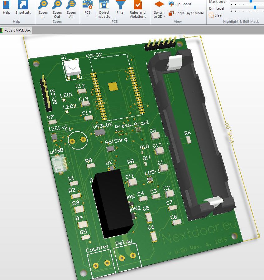
Once the schematic is created, you can place your components on the PCB according to your preferences. The tool also offers auto-routing to build connections without human interaction. This, however, is often – at least partly – done by hand, like you see in the below image, I routed the wires to the relay terminals with a thicker trace.

Once you have all components in place and routing done, you have the option to display your work in a 3D style. This gives you a fairly good idea of what the board will look like and also can serve as an input for engineering the casing of your consumer product.

As you see, most of the components are SMD (surface mounted) devices and such type of parts might require the corresponding soldering technique. Of course, there are some that let you use a conventional soldering iron but really small parts will definitely make it a lot harder to use classic gear with success.
Manufacturability
Finally, it is worth inquiring about physical limits of the machines missioned by the manufacturer of your prototype PCB. Widths, clearances and via sizes are all values you will need to have in mind before sending your plans to production, even for the most simple pieces of work. But in case you get those right, you will have the pleasure of having your own board, custom-built for the very purpose. Like this:

As next, I shall soon continue with the hot air soldering of the above board – then give these four away to my best friends, one of which just promised to tweak it with his kids.